
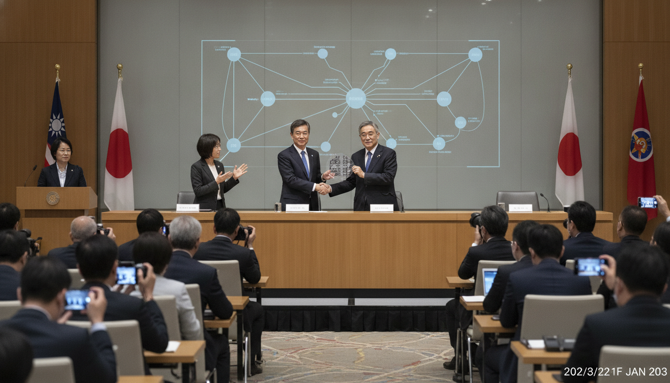
TSMC–Sony Image Sensor Partnership Targets Physical AI Growth
TSMC and Sony partner to produce next-generation image sensors, aiming to capture growth in physical AI as smartphone demand stalls and competition rises.
Taipei and Tokyo — Taiwan Semiconductor Manufacturing Co. (TSMC) has agreed with Sony Group to jointly produce next-generation image sensors, a move the companies say is intended to accelerate growth in "physical AI" applications. The TSMC–Sony image sensor partnership comes as the smartphone market shows limited expansion and regional competition from South Korean and Chinese rivals intensifies. Company statements describe the collaboration as a strategic step to combine Sony’s imaging expertise with TSMC’s manufacturing scale, though the full commercial terms remain undisclosed.
Details of the Joint Production Announcement
TSMC and Sony confirmed they will collaborate on manufacturing advanced image sensors designed for the next wave of AI-enabled devices. The companies characterized the effort as joint production rather than a full merger or acquisition, signaling a partnership focused on combining complementary capabilities. Public announcements did not provide a timetable for mass production, specific investment amounts, or how intellectual property and revenues will be shared.
Industry Pressures Prompt Uncommon Alliance
Analysts say the pact reflects mounting pressure on traditional suppliers as smartphone sales plateau and rivals step up. South Korean firms and domestic Chinese chipmakers have been investing aggressively in imaging and sensor technologies, squeezing margins and market share in segments long dominated by established suppliers. For TSMC, the deal represents an unusual move into optoelectronics production partnerships, prompted by a need to diversify revenue streams amid slower growth in core logic chip demand.
Physical AI as the Strategic Opportunity
Both companies framed the collaboration around "physical AI," a term used to describe devices that combine sensing hardware with on-device artificial intelligence for tasks such as advanced perception, autonomous navigation and real-time analytics. High-performance image sensors are a key enabling technology for those applications, providing the rich, low-latency visual data that edge AI processors require. By aligning sensor development with manufacturing scale, the partners aim to better serve customers building cameras for robotics, automotive systems, smart factories and next-generation mobile devices.
Sony’s Role and Market Strength
Sony remains the global leader in image sensors, with a long track record of supplying high-end camera modules for smartphones and other electronics. The company’s strength in optical and imaging design gives the partnership a technical foundation that TSMC lacks as a pure-play foundry. Sony’s expertise in sensor architecture and pixel performance is expected to guide product specifications, while TSMC brings capacity, process control and advanced packaging know-how to the table.
TSMC’s Strategic Diversification
For TSMC, the agreement marks a notable extension of its business model beyond conventional wafer foundry services. The company has been broadening its offerings into advanced packaging and system-level capabilities, and the sensor collaboration fits into efforts to capture more value across the semiconductor supply chain. Industry observers note that moving closer to component-level production could help TSMC offset cyclical swings in logic-chip demand and deepen relationships with system makers seeking integrated solutions.
Supply-Chain and Regional Competitive Implications
The partnership could reshape competitive dynamics in Asia’s semiconductor landscape by combining a Japanese electronics leader’s design strengths with a Taiwanese manufacturing giant’s scale. That alignment may complicate efforts by South Korean and Chinese firms to displace incumbent suppliers in higher-margin imaging segments. It also underscores wider supply-chain trends toward regional specialization and closer industrial ties across East Asia, where geopolitical and commercial considerations increasingly influence investment decisions.
Key Questions Remain Unanswered
Several practical details remain unclear, including where the joint production will be located, the expected capacity and which customers will first benefit from the new sensors. Observers are also watching whether the partners will target mobile handsets, automotive imaging, industrial vision systems, or a combination of end markets. Regulatory approvals, export controls and intellectual-property arrangements could affect timelines and market access, but both companies so far have limited public commentary on those topics.
Market watchers will be looking for forthcoming technical roadmaps, announced production volumes and pilot partnerships with device makers to assess the initiative’s commercial impact. If the collaboration yields competitive sensor products at scale, it could shift supplier relationships and accelerate deployment of AI capabilities on devices that rely on robust visual sensing.
The TSMC–Sony image sensor partnership signals a strategic shift by major chip and device suppliers toward closer cooperation on hardware that feeds AI at the edge. The combination of Sony’s imaging leadership and TSMC’s manufacturing heft is intended to capture emerging demand for sensors in physical AI systems, but the effort’s success will depend on execution, investment commitments and how quickly the partners can bring demonstrable products to market.

