
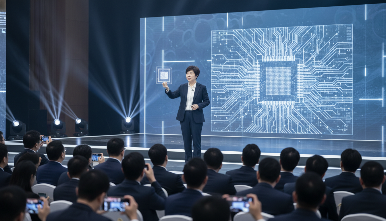
Huawei chip breakthrough: He Tingbo says new design can reduce reliance on EUV tools
He Tingbo says Huawei chip breakthrough can circumvent U.S. export controls and reduce dependence on EUV lithography, shaping global competition.
Huawei’s lead semiconductor executive, He Tingbo, has presented what the company calls a major chip breakthrough that could lessen reliance on extreme ultraviolet (EUV) lithography and blunt the impact of U.S. export controls. The Huawei chip breakthrough was described as a combined redesign of chip architecture and a revised manufacturing pathway intended to keep the company producing advanced products despite restrictions on access to certain tools. The announcement has immediately drawn attention from industry observers, competitors and policymakers assessing how the shift could affect global semiconductor supply chains.
Huawei unveils alternative design and production strategy
He Tingbo outlined a newly developed chip design and a manufacturing approach the company says makes cutting-edge EUV tools unnecessary for its relevant product lines. Huawei describes the work as part of a broader effort to rebuild its semiconductor capabilities after being cut off from some U.S. technologies and suppliers.
Company statements and public appearances by He framed the innovation as pragmatic and defensive: a way to sustain product development and maintain competitiveness without violating export rules. Huawei stressed that the changes were driven by years of internal research and reorganization of its chip teams.
Engineering approach aims at process and architecture trade-offs
According to the presentation, the approach couples modified circuit architectures with process adjustments that rely on existing immersion lithography and multi-patterning techniques. Huawei claims these measures can deliver performance and yield improvements sufficient for its current strategy without immediate access to EUV systems.
Engineers told reporters that the route involves tighter co-design between chip logic and manufacturing process steps, a method that can recover some of the scaling and performance gains normally associated with EUV-based nodes. Huawei’s public remarks emphasized practical product timelines and incremental improvements rather than promises of parity with the world’s most advanced foundries.
EUV dependence challenged but not eliminated, experts say
Huawei’s assertion that EUV tools are unnecessary for its updated product lines has already met cautious responses from semiconductor specialists. Independent engineers note that while design and process work can reduce reliance on EUV for some products, EUV remains central for the most aggressive process nodes used by leading foundries.
Analysts caution that alternative routes can raise production complexity and cost, and may not fully replicate the performance or density of EUV-enabled chips. The long-term viability of Huawei’s pathway will depend on yields, power efficiency and the company’s ability to scale manufacturing without introducing severe cost or reliability trade-offs.
Implications for Taiwan Semiconductor Manufacturing Co. and Intel
Huawei’s announcement is likely to be watched closely by major foundries such as Taiwan Semiconductor Manufacturing Co. (TSMC) and Intel, which operate at the technological edges where EUV is widely deployed. If Huawei’s approach proves commercially viable, it could reshape demand dynamics for advanced tooling and change customers’ procurement strategies.
However, leading foundries retain advantages in process maturity, capacity and the ecosystem of design tools and libraries that support the most advanced nodes. Market observers say any shift will be incremental, with Huawei’s progress judged by demonstrated production runs and the performance of end-user devices using the new chips.
Regulatory and geopolitical ramifications loom large
Beyond engineering implications, the Huawei chip breakthrough raises immediate policy questions for governments applying export controls to slow technology transfers. U.S. and allied policymakers have used restrictions on tools such as EUV lithography to limit the pace at which some companies can adopt cutting-edge manufacturing techniques.
If Huawei can mitigate those constraints through design and process innovation, regulators may reassess the effectiveness of current controls and consider additional measures. Conversely, some officials may view the development as evidence that export restrictions have a limited, medium-term effect on a determined company with deep resources.
Industry reaction and next steps to watch
Semiconductor suppliers, industry analysts and customers are awaiting empirical evidence: independent test results, production yield figures and sample devices that demonstrate the claimed trade-offs. Huawei has said it rebuilt its chip product lines over several years and will publish technical details as conditions allow.
Observers will watch whether Huawei can scale manufacturing, maintain acceptable costs and introduce products that meet market expectations. The company’s ability to certify chips for ecosystem partners and secure supply of specialized materials will also factor into the success of the strategy.
Huawei’s announcement marks a notable moment in the contest over advanced semiconductors, but the real test will be commercial deployment and independent verification. The industry will be monitoring technical disclosures, production milestones and any regulatory responses as the situation evolves.

