
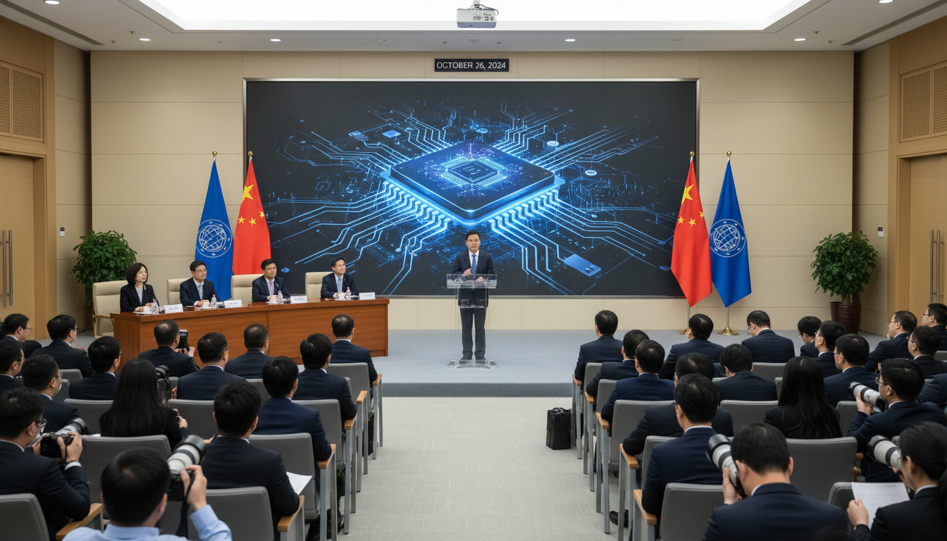
Huawei chip breakthrough: company unveils new design approach to close gap with TSMC and Intel by 2031
Huawei says new chip design method aims to rival TSMC and Intel by 2031 while navigating U.S. sanctions and tight supply chains.
Huawei chip breakthrough claimed on Monday in a statement that the company has developed a novel chip design approach it says could narrow the technological gap with global leaders such as TSMC and Intel by 2031. The announcement, made as the company continues to adapt to U.S. export controls, frames the move as a key step in a multi-year recovery plan for Huawei’s semiconductor ambitions. Company officials said the approach focuses on architecture and packaging innovations rather than relying solely on access to advanced fabrication nodes. The claim adds fresh momentum to a broader effort by Chinese technology firms to reduce dependency on foreign suppliers.
Huawei announces new chip design approach
Huawei said the new approach centers on alternative design and integration techniques that can achieve comparable performance without exclusive access to the world’s most advanced foundries. The company framed the development as a breakthrough in chip architecture, system-level optimization and manufacturing collaboration. Huawei did not disclose all technical specifics publicly, saying only that the method leverages enhanced co-design between chips and software and newly adopted packaging methods.
The statement follows years of investment in in-house capabilities after U.S. measures limited Huawei’s access to high-end semiconductors and design tools. Analysts note the company’s ability to translate design advances into mass-produced, competitive chips will depend on securing a stable supply of wafers, advanced packaging services and lithography equipment. Huawei’s claim, therefore, marks a milestone in design ambitions but does not yet prove parity with foundry-based leaders.
Company sets target to match TSMC and Intel by 2031
Huawei’s public timeline sets 2031 as the target year by which it expects its combined design and manufacturing ecosystem to close much of the performance gap with TSMC and Intel. The company described the timeline as contingent on steady progress in materials, packaging and domestic supply-chain scaling. Executives framed 2031 as an achievable horizon given current investment plans and cooperation with Chinese semiconductor partners.
Industry observers cautioned that roadmap statements are common in corporate strategy announcements and that conversion to market-ready silicon typically faces delays. Matching leading-edge process nodes remains challenging without access to some specialized equipment and materials, they said. Still, the ambition signals Huawei’s intent to be a long-term competitor in high-performance chips and not only in consumer or network devices.
Technical claims and independent skepticism
Huawei has outlined several technical elements of the approach, including system-level architectural adjustments, improved chiplet integration and refined interposer techniques. These methods can improve effective performance and yield benefits in power efficiency and cost at certain scales. The company argued such changes would allow it to produce competitive chips even if it cannot immediately access the most advanced EUV lithography.
Independent analysts urged caution, noting that chiplet and packaging strategies can reduce reliance on leading-edge nodes but do not fully substitute for the raw transistor density achieved by the latest processes. Verification by third-party benchmarks and production-scale yields are the standard measures that will determine real-world competitiveness. Until independent test results or broad customer adoption appear, skepticism will remain part of expert assessments.
Sanctions and supply-chain challenges remain central
Huawei’s announcement directly addresses the fallout from extensive U.S. export controls that have restricted access to advanced semiconductors, development software and certain equipment. Those measures have driven Chinese firms to accelerate domestic research and to develop alternative supply chains. Huawei said its design method is specifically calibrated to operate within those constraints and to make more efficient use of available fabrication options.
However, several critical inputs—advanced lithography, certain high-performance substrates and specialized materials—continue to be sourced globally and are subject to export controls. Industry executives warn that supply-chain bottlenecks and restrictions could slow Huawei’s progress or increase production costs. The path from design claims to resilient manufacturing capacity will require coordination across suppliers and regulatory navigation.
Market reaction and competitor implications
Financial markets and regional semiconductor suppliers reacted with cautious interest to the news, viewing Huawei’s strategy as a long-term factor that could reshape competitive dynamics in Asia. For foundries such as TSMC and established chipmakers like Intel, Huawei’s entrance or acceleration in advanced design could pressure pricing and spur further innovation. Regional ecosystems that provide advanced packaging, testing and substrates may see increased demand if Huawei’s approach proves viable.
For Huawei’s current customers and partners, the announcement raises possibilities for more locally anchored technology stacks and reduced exposure to foreign supply disruptions. It may also prompt competitors and governments to reassess procurement strategies and investment priorities in chip-making infrastructure. The announcement is likely to intensify efforts across the industry to secure supply chains and diversify manufacturing capacity.
Outlook, risks and the road to 2031
Huawei’s stated objective of narrowing the gap with TSMC and Intel by 2031 establishes a clear timeframe for measurement, but the company faces several critical tests ahead. Demonstrating consistent production yields, achieving comparable benchmark performance and securing wide customer adoption are the key milestones analysts will watch. In addition to technical hurdles, geopolitical factors and export controls will shape how quickly Huawei can scale its ambitions.
The next 12 to 24 months will be pivotal: measurable silicon demonstrations, third-party testing and supply-chain agreements would lend credibility to Huawei’s claims. Conversely, continued restrictions or setbacks in manufacturing partnerships could extend timelines beyond 2031. Observers say the industry should expect an incremental progression rather than a sudden leap, with each technical and commercial success narrowing the gap.
Huawei’s announcement on May 25, 2026, underscores the company’s strategic pivot toward design-led innovation and integration as a response to external constraints. Whether the “Huawei chip breakthrough” becomes a widely accepted industry reality will depend on tangible outcomes in performance, production and market adoption over the coming years.

