
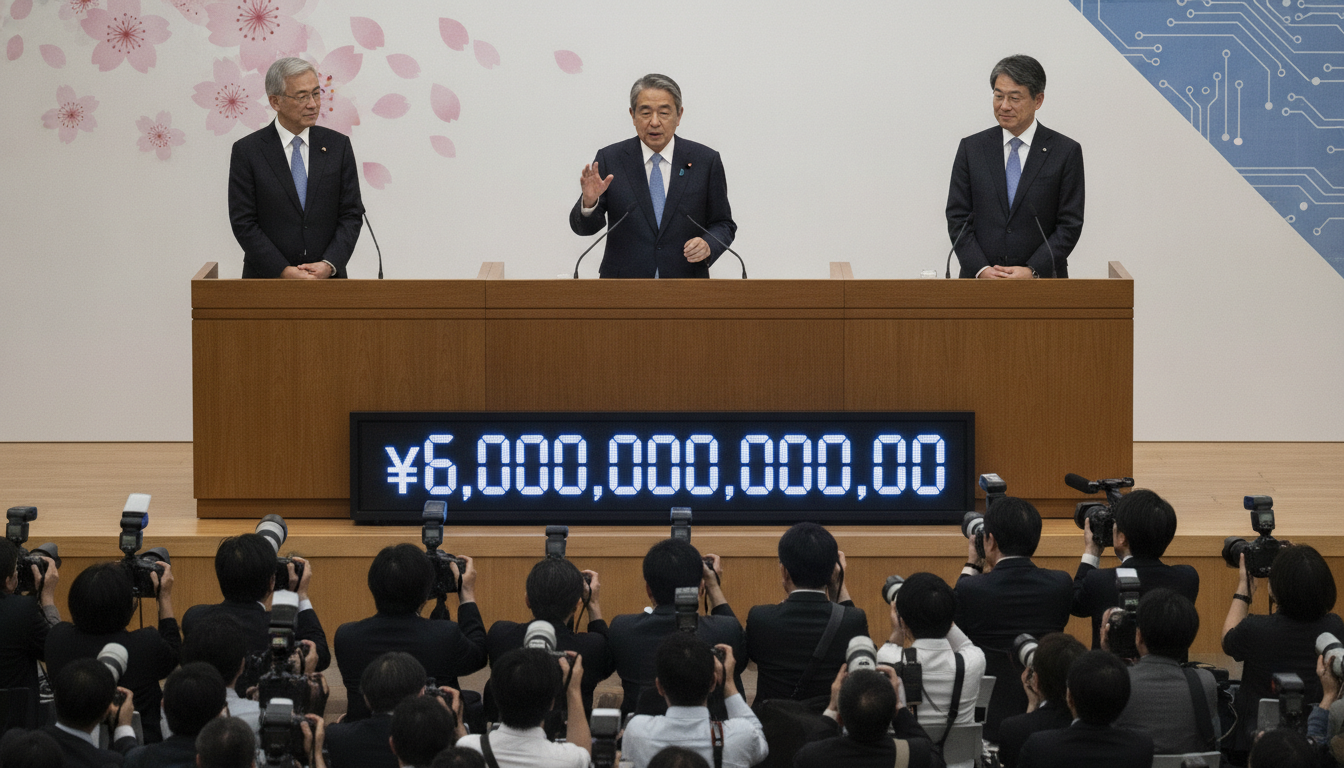
Japan chip investment climbs to 6 trillion yen after Sony and TSMC announce image sensor plant
Japan chip investment climbs to 6 trillion yen as Sony and TSMC announce an image sensor plant, underscoring Tokyo subsidies and mounting global tech demand.
Japan’s chip investment has surged to 6 trillion yen following a joint announcement by Sony Group and Taiwan Semiconductor Manufacturing Co. that they will build a new image sensor plant in Japan. The move marks a significant boost to efforts to revitalize domestic semiconductor capacity and aims to attract further foreign capital into the country’s technology ecosystem. The announced investment comes amid intensive competition for global chip manufacturing between Asia and the United States.
Foreign investment in Japan’s semiconductor sector totals 6 trillion yen
Japan’s latest tally of foreign-led capital commitments to its semiconductor industry now stands at roughly 6 trillion yen, or about $37 billion. That total reflects a string of investments by major foundries and equipment suppliers, capped most recently by the Sony-TSMC image sensor project announced in August 2026. Officials and industry executives say the inflow reflects both market demand for advanced sensors and strategic efforts to onshore supply chains.
The figure also illustrates how global supply-chain realignments and geopolitical considerations have encouraged companies to diversify production away from single-region concentration. Investors have cited demand from automotive, smartphone and artificial intelligence applications as primary drivers for expanding capacity in Japan.
Sony and TSMC detail image sensor plant partnership
Sony and TSMC said the new plant will focus on advanced image sensors, a segment where Sony has long held market leadership and TSMC brings high-volume manufacturing expertise. Company statements described a collaboration that pairs Sony’s sensor design capabilities with TSMC’s wafer fabrication scale and process technologies. The partners did not disclose full financial terms beyond confirming the project’s material contribution to the broader investment total.
Industry sources indicate the plant will be built near existing supply-chain hubs to streamline logistics and take advantage of skilled local workforces. Plans are expected to unfold over multiple years with phased capacity additions aimed at meeting rising demand for high-performance sensors in mobile devices, automotive cameras and data-center AI applications.
Tokyo subsidies and policy incentives behind investment wave
The Japanese government has actively sought to attract semiconductor investment through direct subsidies, tax incentives and regulatory support. Tokyo’s package of incentives—ranging from grants for capital expenditure to favorable land and permitting arrangements—was cited by both international and domestic executives as instrumental in their decisions to expand in Japan. Officials argue these measures improve the economic viability of building complex fabrication facilities domestically.
While subsidies reduce initial cost burdens, analysts say companies also weigh broader factors such as proximity to customers, workforce availability and political stability. The government’s semiconductor strategy aims to balance short-term inducements with longer-term commitments to research, workforce training and local supplier development.
U.S. tech and AI companies continue to exert pull on global investment
Despite Japan’s incentives, U.S. technology and artificial intelligence firms remain powerful magnets for chip manufacturing and related investments. Major U.S. cloud providers and AI hardware buyers continue to place large, long-term orders that influence where fabs and packaging lines are sited. These commercial relationships often lead chipmakers to cluster around data-center regions or to pursue capacity where large, repeatable orders justify significant capital expenditure.
Executives say that while Tokyo’s subsidies are competitive, many decisionmakers also prioritize access to anchor customers and integrated ecosystems. As AI workloads grow and chip designs diversify, the dynamics of demand will remain a key determinant of where future capacity is built.
Regional impact and supply-chain benefits for Kumamoto and beyond
The new investments are expected to produce pronounced regional effects, particularly in areas where fabs and assembly plants are sited. TSMC’s earlier investments in Japan—totaling substantial sums across multiple facilities including those in Kumamoto prefecture—have already generated jobs and stimulated demand for local suppliers. The Sony-TSMC project is likely to expand subcontracting opportunities for equipment makers, chemical suppliers and logistics providers.
Local authorities and business groups project that enhanced semiconductor activity will spur infrastructure upgrades and workforce development programs. However, stakeholders also note the need for sustained collaboration between central and prefectural governments to ensure that training pipelines and support services keep pace with technological demands.
Industry outlook and risks for Japan’s semiconductor ambitions
Analysts see Japan’s expanded investment footprint as a strategic positive but caution that execution risks remain. Building and ramping advanced semiconductor plants involves long lead times, technical complexity and exposure to cyclical demand swings. Supply-chain bottlenecks for specialized tools and materials could constrain timelines, while shifts in global demand patterns might affect utilization rates once capacity comes online.
Nevertheless, the aggregation of large-scale investments—coupled with government support and established electronics expertise—gives Japan a stronger platform to capture a larger share of the semiconductor value chain. Companies and policymakers will need to coordinate on workforce development and supplier resilience to translate financial commitments into sustained production capability.
The Sony-TSMC image sensor project, together with prior foundry investments, reinforces Japan’s re-emergence as a focal point for semiconductor manufacturing in Asia. Continued attention to commercial partnerships, supply-chain depth and long-term policy stability will determine whether these investments become a durable cornerstone of Japan’s technology sector.

